
- Campus , Education , Research
- 31/01/2024

Cleanroom tour aims to open eyes
TU/e’s best-kept secret, the cleanroom Nanolab@TU/e in the Spectrum building, needs more publicity. So says professor Erwin Kessels, who invited communication staff and student information officers for a tour. In the only cleanroom of Applied Physics & Science Education you can see how chips are made. Cursor tagged along.
I have never written on paper quite as special as what I’m taking notes on this Monday afternoon. It’s light blue and incredibly smooth. It’s the only paper allowed to be taken into the cleanroom, because its fibers won’t release and float through the air.
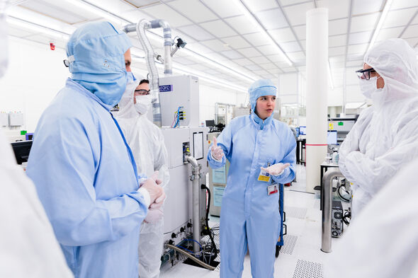
Completely covered from head to toe, we get to look at the expensive equipment accumulated there over the years. The Nanolab has been around for two decades and there are already new visions for the future. In two years, it will be an independent part of the yet-to-be-built ASML cleanroom and it will be expanded to one and a half times its size. “It’s already a gem,” says Erwin Kessels, Professor of Plasma & Materials Processing, who knows that colleagues from all around the world are amazed by it, “but it can become even more beautiful.”

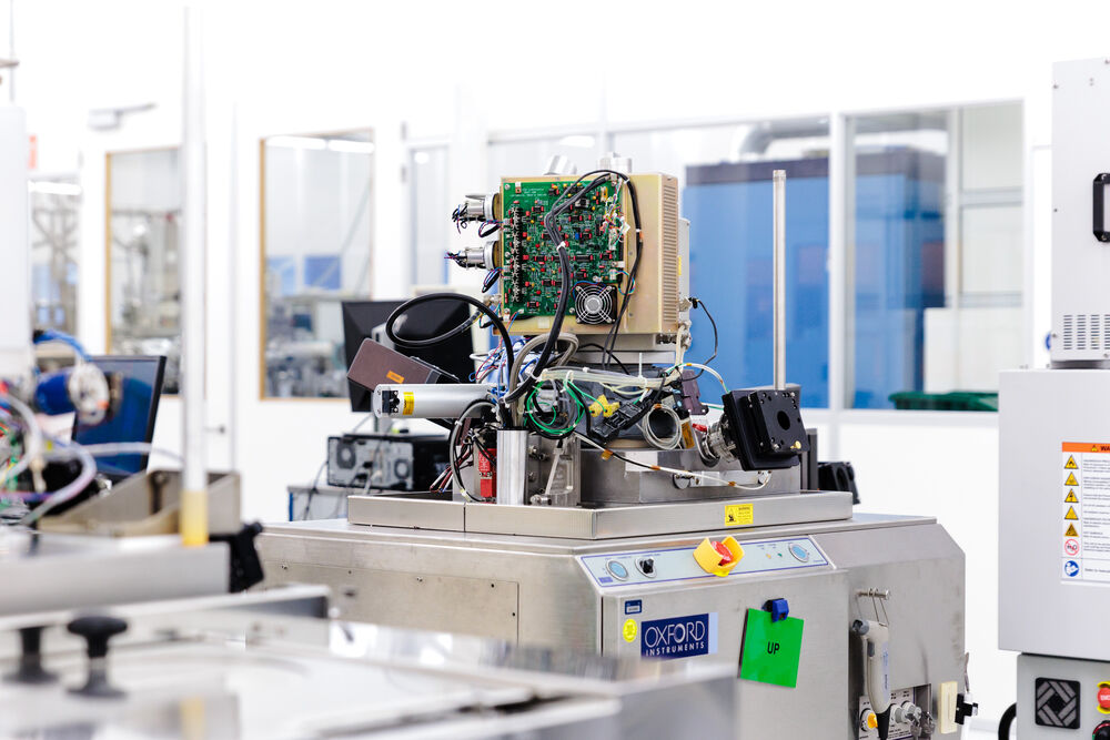
When we get to the machine that can perform deposition and etching techniques, which were explained to us during the introduction at Flux, Kessels reveals that it cost about a million euros. “But what an ugly piece of machinery. For that kind of money, couldn’t they have paid some more attention to the design?” says communications officer Cindy de Koning. “What’s important to us is that we can see what happens inside it. It certainly gets our hearts racing,” Kessels replies promptly.

We briefly linger at all the equipment and facilities: the ion accelerator, the special microscopes for examining wafers, and the lab for “wet chemistry”. Kessels had already told us about the five steps in chip manufacturing; now we can see firsthand what the process entails. It’s impressive, as is the temperature (a constant 21 degrees) and the noise from the ventilation.
How do you keep a cleanroom clean, someone asks. The air flows downwards in “down flow” and is forced through the holes in the floor tiles. We also get to take a look in the basement, which is not only the place where that air is filtered, but also where any residue from the gases used in evaporation is removed. And the laser light is made here. Don’t ask me how.

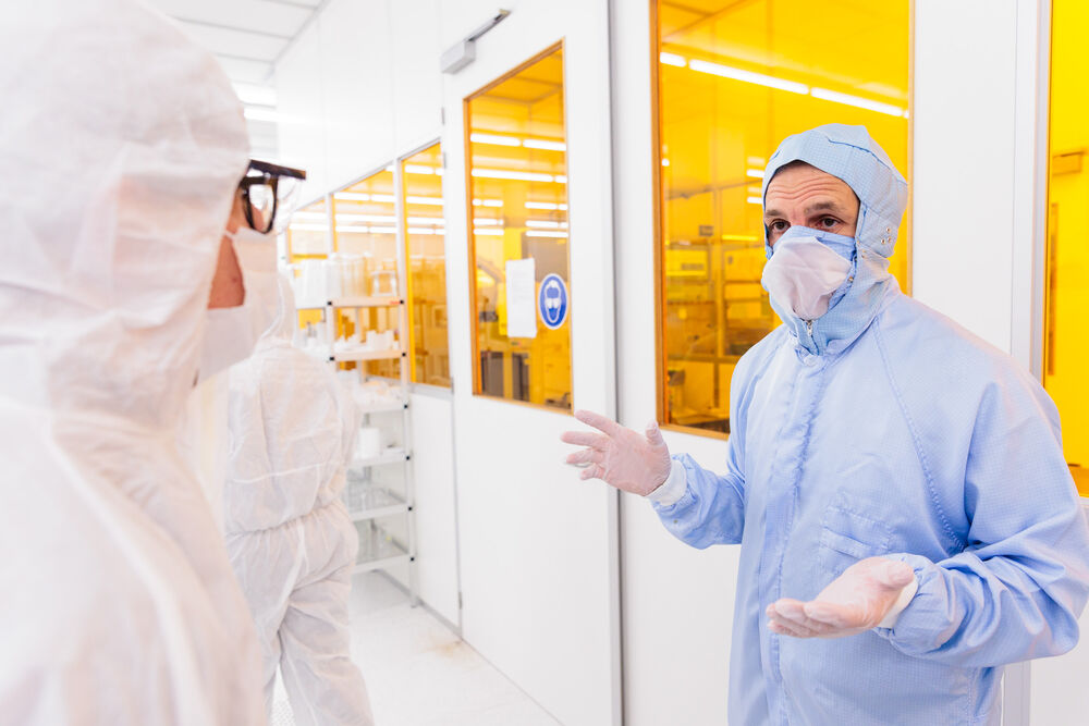
The lab needs more recognition, student Mick Gielen and lecturer Harm Knoops agree. Gielen was the one who came up with the idea for the tour. “The fact that we can manufacture chips here in the Netherlands is of great importance, on a geopolitical as well as an economic level. I would like secondary school students to be informed of what you can learn about semiconductor-related research at TU/e,” says the member of the student information team.
Lecturer Knoops calls himself a “child of the region”. He is a TU/e alumnus, is currently working at Oxford Instruments and teaches physics students for one day a week here. “The trends in chip making are that everything is getting smaller, more 3D techniques are applied and more and more materials are used.” Those trends can be observed if you read Kessels’ blog on Atomic Limits, a website for experts in the field.
Chips are needed for data storage, Artificial Intelligence, Internet of Things, 5G communication and Automotive. Although this will certainly appeal to secondary school students, what they may not realize is that Applied Physics & Science Education is the place to be if you’re looking for a program in those fields. We have definitely been convinced of that this afternoon.
Discussion