
- Research
- 10 min
- 28/02/2018

The new Brainport Gold
Some people regard it as the new gold for the Eindhoven region. For nowhere in the world have people progressed this far with the development of the optical chip, which is to change the world in the years to come. Faster and more energy-efficient Internet traffic, innovative health sensors and safer aviation; these are just a few examples of areas in which integrated photonics is going to make the difference in the next few years. TU/e is the front runner in the field of photonics research and is at the cradle of various successful startups that will take the optical chip to the market.
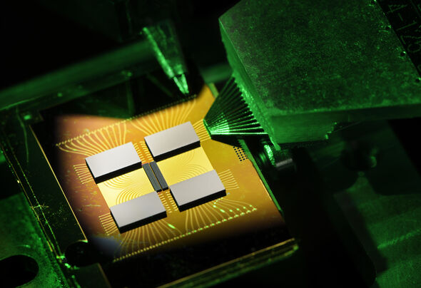
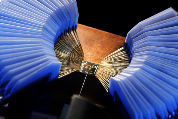
A chip that works with light - photons - instead of the standard electrons as information carrier. These photonic chips the size of a grain of rice are built into increasing numbers of devices and are going to bring about a new revolution, if we are to believe Ton Backx, CEO of the Institute for Photonic Integration.
For the handling of data traffic in 2016 over five percent of the total electric power was consumed worldwide. And this use is growing at an exponential rate. We want to exchange ever more information with our mobile phones and many devices are also connected with the Internet more and more often. Not to mention the data flow required for the intercommunication between the devices. The electronic superhighway is getting congested and in order to prevent that, we will need to switch to new technologies. And we do not have to look far, says professor Ton Backx with enthusiasm. He is the director of the Institute for Photonic Integration (IPI) that was set up in 2016 and that pools knowledge in the field of integrated photonics.

“There are two problems we are coming up against in today’s data traffic. On the one hand, the microelectronics being used today has reached its limits if you consider the efficiency of data processing. On the other hand, the energy consumption needs to be cut back drastically if we want to continue in this way. That is why we are working hard here to put the integrated photonic chip on the market.
Communication by means of light harbors a number of major advantages. Photons are massless so that they can move relatively quickly. And they have no charge, so that there is no energy loss occurring to the environment. By means of photons many processes can become far more energy-efficient. Moreover, optical components fit onto a much smaller chip, which makes them simpler to integrate and which makes the optical systems far less sensitive to environmental influences. At the highest transport levels most of the communication is already taking place via light traveling through optical fiber cables. Now we are going to extend that to all the other layers.”
The fact that Eindhoven has taken the lead in the field of integrated photonics is the result of a long history in which - hardly amazing - Philips plays an important part. As early as in the mid-1960s Philips developed optical fiber technology for telecommunications and later it used the light-based technology also for the storage of data on CD, DVD and Blue Ray. Although Philips had always played a leading role, TU/e was involved in this at an early stage. This ultimately resulted in a strong knowledge position, which gave rise to various startups and research institutes IPI and Photon Delta. Backx explains that an ecosystem like Photon Delta, in which companies can participate also, is essential. “We are at a critical moment today. The infrastructure needs to expand at a rapid pace so that we can take the next step required to convert developments into scalable market models. Whilst the government is aware of the importance of photonics, it should do more than just pay lip-service. Sizeable investments are needed for both applied and fundamental research.”
According to Backx there is a great deal of knowledge and plenty of application-oriented developments ready to be brought into the market before long. “Initially the transition to optical chips is occurring in the areas of data and telecommunications. Even today, transceivers are being used that are largely based on optical technology.
And the new mobile 5G network will be made possible by integrated photonics as well. This technology is bound to change the world and will help solve many of today’s societal challenges. Precision robots operating from a distance, medical sensors, extremely accurate optical ultrasound variants which will enable us to distinguish the minutest details in 3D tissue structures, to watch even the metabolism within cells. Self-driving vehicles, smart city developments, the sensor technology required to keep large cities viable, by controlling the quality of water and air. All of this is being developed today, on a photonics foundation. This is a next-generation basic technology on which we will be able to build many more things. How magnificent can it be that we in Eindhoven can lead this effort.”

Photonics @ TU/e
Integrated photonics is the answer for the transport of the growing amount of data. TU/e is leading the way in this research.
The Eindhoven top formula
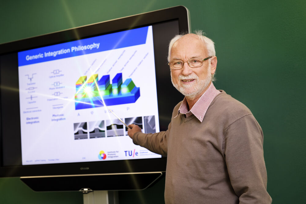
“There is a revolution about to take place in the field of photonics like the one we saw in the 1970s with the emergence of microelectronics,” Meint Smit, Professor of Photonic Integration, assures us.
“Thanks to the photonic integration technology that we have developed in the Netherlands over the past few decades, we are eminently positioned for that revolution. Ever since the 1980s the Netherlands has been investing in research into photonic materials, components and systems. That is a very strong combination indeed. As a result, we have developed a standardized integration process, in which you can merge optical building blocks to form all sorts of functional circuits. Since 2007 we have opened up this integration process for input by other universities. By combining several designs on one wafer we were able to reduce the development costs of chips significantly, thereby making them affordable for smaller companies as well.”
“Since 2013 this process has been commercialized by Smart Photonics, a startup that has emerged from our group. Within it, chips are being developed by a number of enterprises, including two other startups from our group, Effect Photonics and Bright Photonics. We ourselves are now working on the development of new processes featuring even better properties. And we are also looking into their integration with electric circuits, so that in the future we will be able to make a chip that encompasses everything. Cooperation with other sections is of the essence here, for that chip needs to be controlled and end up in an attractive little box, if you want to use it at all.”

From material to large-scale production
“Fifteen years ago you had just got your first mobile phone and if you see today what you can do with your smartphone… Initially these innovations are all electronics-driven. Now that the challenges lie mostly in the area of data transportation, we need to explore other avenues and are making increasing use of photonics to cope with the growing data flow”, says Erwin Kessels, Professor of Plasma & Materials Processing; Academic Director of NanoLab@TU/e.
“With our research into materials and the development of new material systems we are at the innovative basis. Thus, we are working on nanolasers that will be used in optical chips; which materials are the most suited for making these lasers? Can we use nanowires, for example? And if so, how can we position them best so that we incur the least possible loss; and with what material should we encase them?”
“We are also looking into the use of so-called two-dimensional materials like graphene, which have extraordinary electronic and optical properties. We try to involve the business community at an early stage in the technological development and to have them invest in new production equipment. For it may be very nice that you can develop a device in a lab, but at the end of the day you need equipment to be able to produce it on a large scale. We try to set up the entire chain here, from material to production facility.”

5G internet: fast and safe
“For the support of the new generation of mobile networks, 5G, we use wireless systems with photonics lasers. A new generation of antennae with targeted bundle steering, receivers, transmitters, signal processors; it is quite a system that is going to run partly on photonic chips and in which the connection between photonics and electronics is essential as well”, says Idelfonso Tafur Monroy, Director of the System Integration Technology Center.

“For good systems you need good components and chips, and for those you need good materials. With high-tech facilities, excellent knowledge and cooperation with enterprises we are positioned in a unique triangle. We also see this reflected in the Flagship Telecom 5G, in which together with the business community we are developing high-quality technology. Which is good for students, too: future testing grounds with 5G on campus.”
“Due to the development of superfast Internet the data flow is growing exponentially. Especially when before long – also thanks to photonics – we are going to use all kinds of health sensors every day and use self-driving vehicles. Of course, the data involved will need to be transported safely. That is why we are also working on quantum cryptography whereby strands of photons provide unhackable communication. New technology will have to be fast, but also safe in particular.”
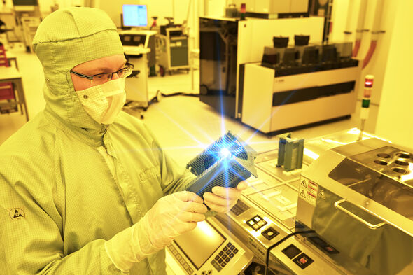
Cooperation in unique cleanroom
“With our NanoLab@TU/e we possess a unique facility where university and the business community merge. The combination of state-of-the-art machinery with high-tech lithography equipment like an ASML DUV scanner, and the presence of a permanent staff with a great amount of expertise definitely contributes to our leading position in the area of indium phosphide (InP) photonics.”
Huub Ambrosius, managing director NanoLab@TU/e: “Although it is a technology that is still in its infancy, applications for it will be legion within the foreseeable future. Not only in the world of telecom and data centers, but especially for everyday use in and around the house.
Therefore we need to ensure that we develop the technology further in such a way that we can go and make chips with a high yield and at low costs. This makes it essential to cooperate with enterprises that develop and produce machinery and components of it. In addition, we are working actively on the next generation of chips, a combination of photonics and electronics. There, too, we can make the difference.”
“Around us considerable investments are being made on various fronts. Thus, the Institute for Compound Semiconductors of Cardiff University (UK) is currently building an ultramodern big cleanroom, using an investment of dozens of millions. We need to jump on the bandwagon, companies and governments must be shaken awake. We should not only keep shouting that this place is great, now is the time to act vigorously. Otherwise they will pass us by before we know it.”

Bringing a smart chip into the market
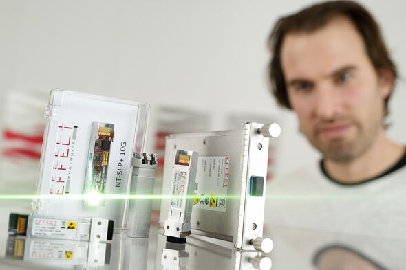
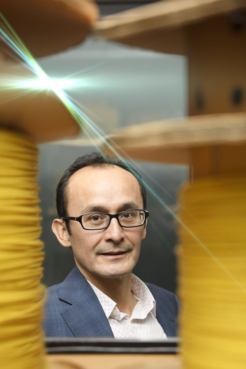
“During my statutory PhD period at TU/e in the group of Meint Smit I noticed that the splendid technology developed within the labs usually stays there. The business community hardly makes any use of this knowledge and we intend to change that with the foundation of Effect Photonics - now seven years ago”, states Boudwijn Docter, CTO Effect Photonics.
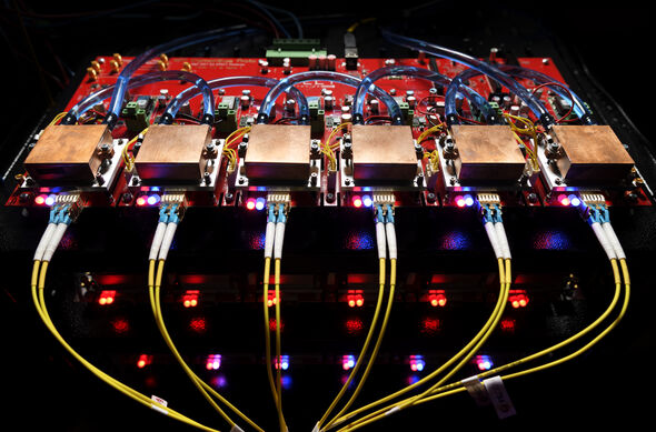
“We make components for optical fiber networks on the basis of optical chips which have their origin at TU/e and which we are now developing further. A box with an optical fiber connector on the front, an electric connector on the back and an optical chip inside with all the optical functions integrated into it. That is how we provide our modules to clients such as Nokia and Ericsson.
And they want more. The quantities of gigabits transmitted per second increase exponentially, so new technology is absolutely needed to keep up with the rapid processing of the data flow. Given the Internet of Things coming on full tilt, whereby ‘smart’ devices will themselves start communicating with the Internet, the pace is picking up even more. Whereas consumers can see that there are all sorts of new applications coming up, the big masses are not particularly interested in the fact that those applications are running on integrated photonics. Even though life without them is almost impossible by now.”
“For the production of our optical chips we are cooperating closely with Smart Photonics, another TU/e spinoff. A design can be optimized efficiently once you have insight into the production process, and this is how we hope to speed up the maturity of the market. Together with Ton Backx from Photon Delta we are putting a photonics ecosystem on the map. And that is a dire necessity, certainly if you want to secure big investments.”
Optical chip made of small building blocks
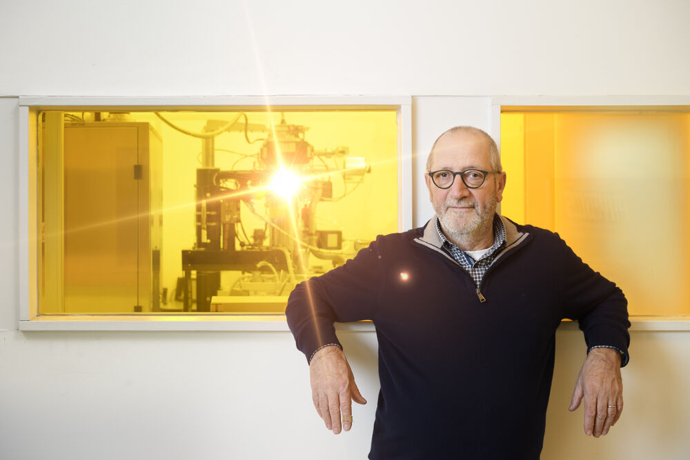
“At the moment things are moving very fast in the world of integrated photonics. As early as next year optical chips from Eindhoven will come onto the market that will make the difference in the Telecom branch”, says Luc Augustin, CTO Smart Photonics.
“Initially these optical chips will be used for long-distance communication between data centers. While consumers may not notice this at once, if we do not make this step to optical chips, the Internet traffic could not maintain the same speed.”
“SMART Photonics produces optical chips on the basis of a unique generic integration process, developed by us and TU/e jointly. We provide small building blocks and customers can connect these themselves and thus design the required functionality. A laser, light detection or filtering? Even without extensive knowledge of semiconductor materials it is possible for customers via this route to design optical chips themselves.”
“For now we are in the lead, because we are holding a unique technology. Globally the focus is on silicon photonics whereby you can use the current electronics infrastructure. In Eindhoven we do not work with silicon, but with indium phosphide as the basic material. For many years already this material has proven its reliability in telecom, and unlike silicon, you can build lasers into it. Which makes it extremely efficient: the production of photonic chips without a light source is like the building of a car without an engine. So we have an excellent hand indeed, but if we are to win the ultimate battle, more investments are needed. The rest of the world is not sitting idly by.”
Tomorrow’s measuring instruments
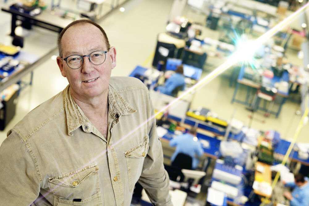
“Technobis is the first and so far only company that is commercially marketing sensors based on integrated photonics”, Pim Kats states. He is the CEO of Technobis.
“At some time we started with fiber measuring instruments, which can measure pressure, tension and temperature. However, at a very low resolution you cannot get away with classical optics anymore and after talking to TU/e Professor Meint Smit I understood that we had to change course towards optical chips. There is no end of applications. For Airbus we are developing measuring systems that display forces on the landing gear during landing and take-off, and sensors enable us to measure minute metal fatigue.”
“Everybody is getting convinced that these are tomorrow’s measuring instruments: lightweight, micro size and highly energy-efficient. Apart from aviation, there are numerous medical applications for our sensors. Thus, they are integrated into catheters and endoscopes to perform all kinds of measurements during surgery. And they are being used in the world of racing, for instance to measure pressure, vibrations and combustion in Formula 1 cars. In about ten years we can expect these sensors in every new passenger car produced.”

“Integrated photonics is an unstoppable novelty that is going to cause major breakthroughs. And we are contributing more than a fair share to that. Jointly with TU/e we are developing the next generation of chip components, of which we are producing packages on an industrial scale that will have to be affordable.”
Discussion